
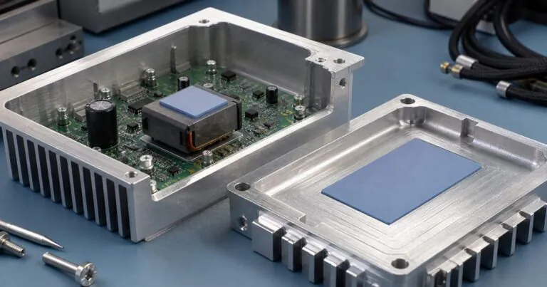
A PCB may fit an aluminum enclosure while its hottest component still has no reliable path to the enclosure wall. For engineers developing sealed controllers, communication modules, or compact power electronics, the gap between a device and the housing affects both heat transfer and mechanical assembly. A pad chosen only by nominal thickness can lose contact or place unwanted force on the board.
Design the interface as a complete path from the heat source through the pad and aluminum wall to the surrounding environment. This guide explains how to map the path, calculate the gap range, compare enclosure structures, specify the contact surface, and validate a representative prototype before releasing a repeatable drawing.
Why does the complete heat path matter more than the pad alone?
A thermal pad can help bridge a controlled gap, but it cannot correct an unsuitable path from the component to the outside air. The electrical package, PCB, pad, enclosure wall, mounting arrangement, and surrounding conditions all affect the result. Thermal resistance is therefore a property of the assembled path, not simply a number on a pad datasheet.[1][2]
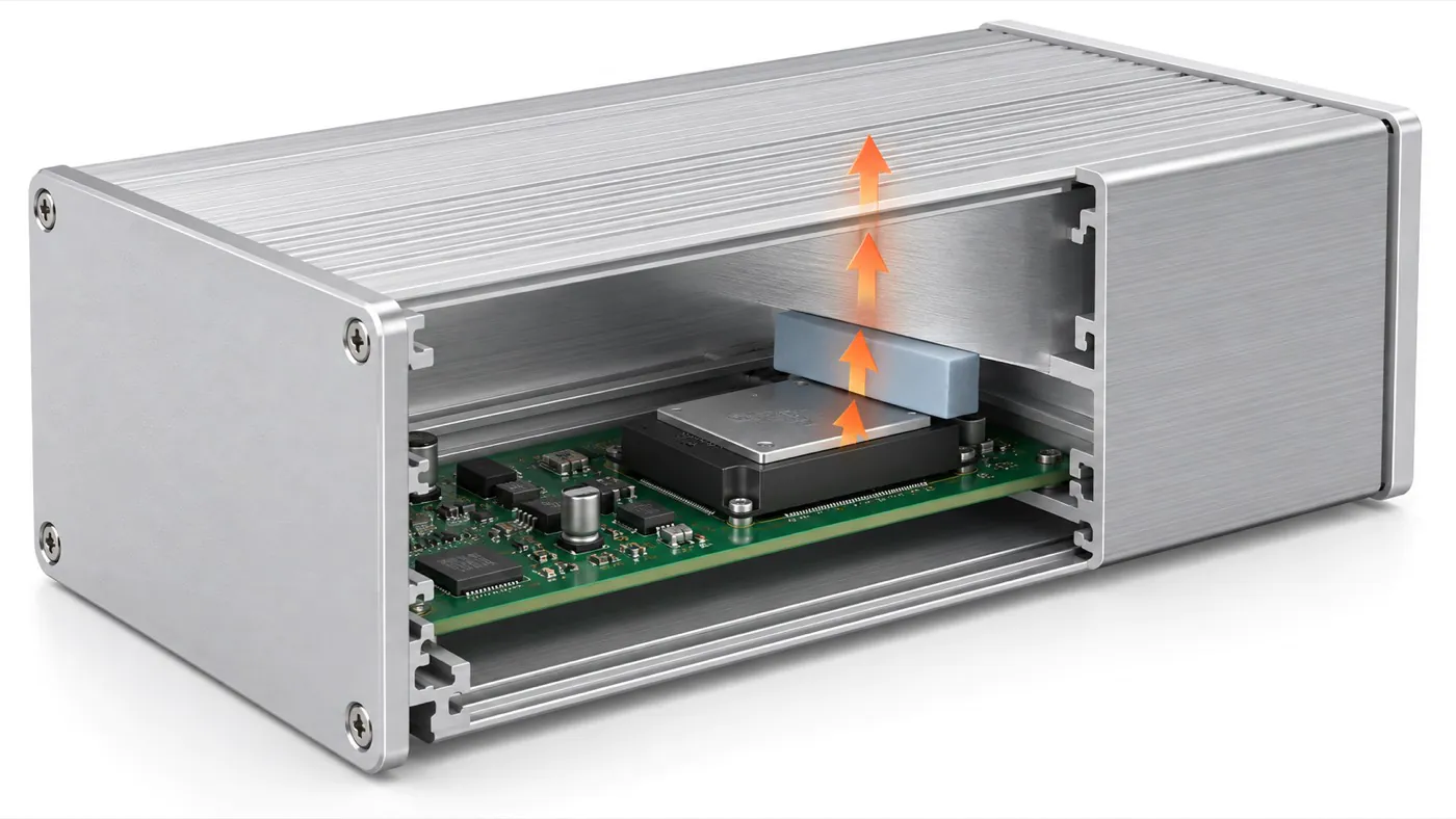
A continuous contact path is needed before the enclosure can spread heat.
- Identify the actual heat source. Use the component and PCB team's power estimates and temperature limits. A visually large component is not necessarily the dominant thermal load.
- Map every interface. Include any device package, spreader, PCB copper, pad, wall, and external surface in the review. A gap or weak contact at one interface can dominate the path.
- Check where heat leaves the enclosure. Wall area, mounting surfaces, airflow, orientation, and nearby equipment change the final boundary condition. An aluminum wall alone does not establish a safe component temperature.
- Assign validation to the system owner. The enclosure supplier can assess machinable contact features and drawing requirements; the electronics team must confirm powered-system temperatures under representative conditions.
For an existing extruded aluminum enclosure profile, first check whether the wall and PCB positions permit a practical contact path. An existing profile is a useful starting point only when its available geometry suits the project.
Statement: A pad with a favorable datasheet conductivity guarantees acceptable component temperature inside an aluminum enclosure.
Answer: False
Explanation: Datasheet properties do not capture the complete contact path or the device's operating environment; the assembled system needs verification.
What dimensions should define the thermal gap?
Define a minimum and maximum assembled gap at each intended pad location, rather than using only one nominal value. The range should include PCB thickness and position, component height, standoff or rail position, enclosure-wall location, and the tolerances of parts that set the stack.
| Dimension or condition | Information to request | Why it changes the interface |
|---|---|---|
| Heat-source top surface | Component drawing and mounted height | Establishes one side of the gap; package variation can change contact. |
| PCB location | Board thickness, rail or standoff geometry, and mounting datums | Controls the heat-source position relative to the wall. |
| Enclosure contact land | Section drawing, wall location, and local flatness requirement | Defines the other side of the gap and usable pad area. |
| Closing condition | Fastener locations, closure sequence, and nearby connectors | Can change deflection, contact pressure, and connector alignment. |
| Pad after installation | Candidate material datasheet and allowable assembled thickness | Determines whether the candidate can conform without excessive force. |
- Calculate both gap extremes. A pad that touches at the tightest stack may fail to contact at the widest stack. Review both before selecting thickness.
- Use functional datums. Relate the contact land to the PCB-support features on one controlled drawing. Independent nominal dimensions may conceal a large stack variation.
- Protect the PCB and connector fit. Excessive compression can load the board or move a connector relative to its panel opening; insufficient compression can leave a weak thermal contact.
Material suppliers publish product-specific guidance for compression and thermal performance. Apply the limits of the actual candidate pad rather than a universal compression percentage.[1]
Statement: The nominal distance from a component to an enclosure wall is enough to specify a thermal pad.
Answer: False
Explanation: The assembled minimum and maximum gaps determine whether the pad can make contact without imposing excessive force.
When can an existing extrusion support the required contact geometry?
An existing extrusion can work when its PCB rails, internal wall, and available machining area align with the heat source and required pad footprint. It should be evaluated against the PCB and thermal stack before promising a faster development route or avoiding dedicated tooling.
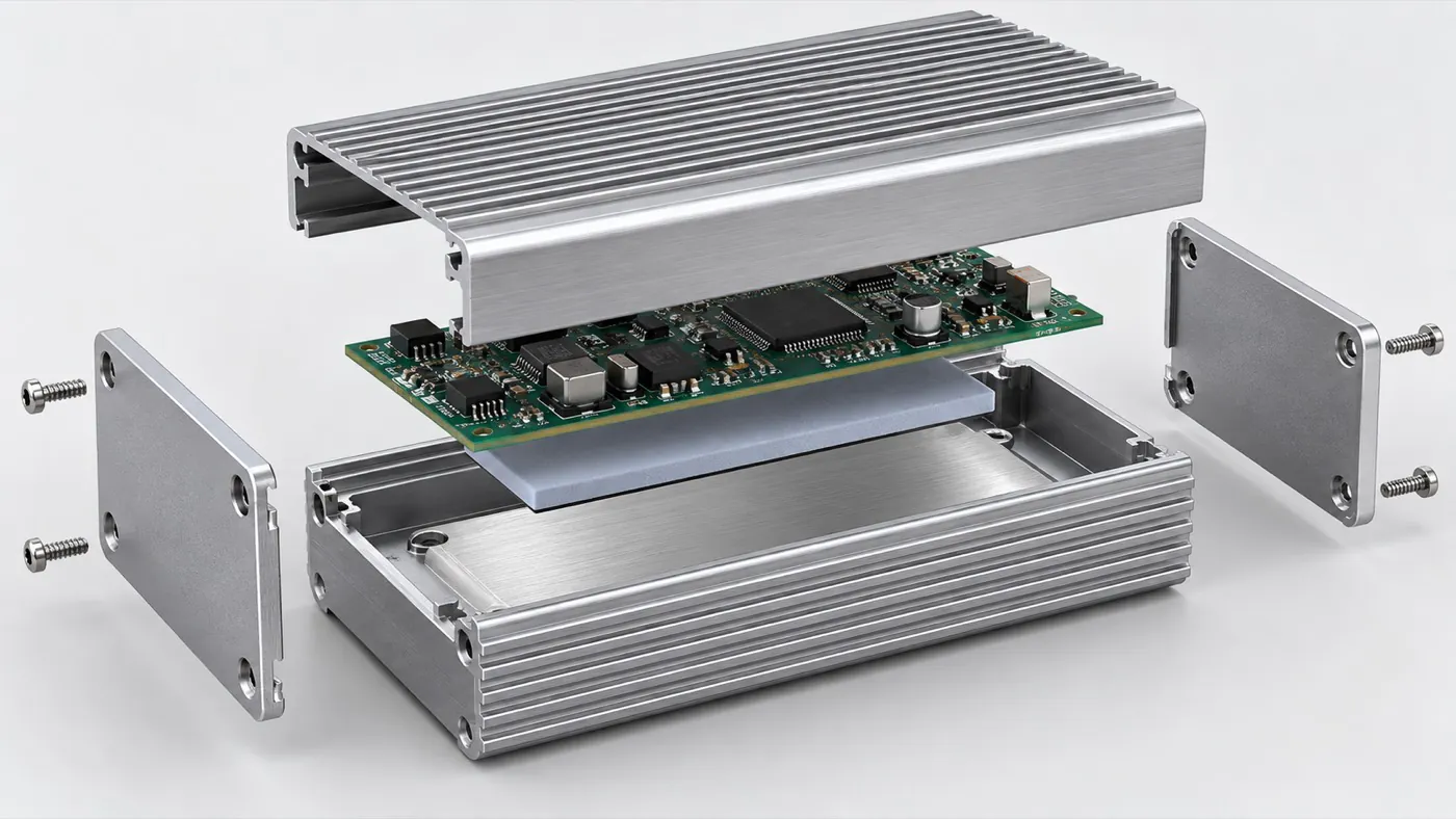
Existing profile features help only when they meet the project's contact and assembly needs.
- Check the usable wall region. Screw channels, end-panel grooves, or internal ribs may interrupt the intended contact land.
- Compare PCB support positions. A profile with suitable exterior size may still locate the board too far from the wall for the chosen pad.
- Evaluate local machining. A CNC-machined flat land or suitable feature may improve contact if there is sufficient material and the selected profile permits the operation.
- Escalate when the geometry does not fit. If the heat source, enclosure form, or wall thickness cannot be reconciled, assess another profile or a dedicated manufacturing route rather than forcing an unsuitable pad stack.
The enclosure choice should also accommodate connector openings, mounting requirements, and any finish constraints; a thermal improvement that prevents practical assembly is not a workable solution.
Statement: Every standard extruded enclosure can be adapted to any thermal pad location by CNC machining alone.
Answer: False
Explanation: Available wall material, profile geometry, PCB position, and machining access limit the adaptation options.
How should engineers compare pad materials and contact conditions?
Compare candidate pads at the project's final assembled thickness and contact conditions. Bulk conductivity alone is an incomplete selection criterion because surface conformity, pressure, electrical requirements, aging, and handling also matter.[1]
| Selection factor | Project question | Decision to document |
|---|---|---|
| Thermal performance | What resistance does the supplier report at the relevant thickness and pressure? | Candidate material and test basis. |
| Mechanical loading | What force reaches the PCB, solder joints, and fasteners? | Acceptable compression and support arrangement. |
| Electrical behavior | Must the interface remain electrically insulating? | Material and spacing requirements. |
| Surface conformity | Are the mating faces flat, rough, stepped, or finished? | Contact-land preparation and acceptance method. |
| Service conditions | Will the product be reopened, vibrated, or used over a broad temperature range? | Replacement and validation plan. |
- Use the pad maker's data. Supplier test methods and pressure conditions may differ; ask for data relevant to the installed state.
- Check the final finish. The contact area and finish stack can affect fit and contact. Specify any area that must remain suitable for the chosen thermal interface.
- Avoid a single-material assumption. A softer pad may reduce mechanical loading but may have different thermal or durability behavior; compare the complete requirement set.
The electronics team should approve electrical insulation and thermal material selection. PUMAYCASE can review the enclosure features and manufacturing information needed to implement the chosen interface.
Statement: The pad with the highest advertised bulk conductivity is always the best choice for an enclosure interface.
Answer: False
Explanation: Installed thickness, contact pressure, mechanical load, electrical requirements, and service conditions can change the appropriate choice.
Which enclosure drawing details prevent thermal-interface rework?
Put the thermal contact area, PCB-support datums, and panel interfaces on controlled drawings so the sample and repeat orders are assessed against the same geometry. The drawing should describe the enclosure features the supplier can make and inspect, while the customer keeps ownership of powered-device validation.
| Drawing item | What to show | Review purpose |
|---|---|---|
| Contact land | Location, usable footprint, and project-specific surface requirement | Confirms the pad has a suitable mating region. |
| PCB support | Rails, standoffs, fastening points, and functional datums | Controls the thermal gap stack. |
| Nearby features | Connectors, cutouts, fasteners, and keep-out areas | Prevents interference and assembly stress. |
| Revision control | Part number, drawing revision, and approved sample reference | Supports pilot builds and repeat supply. |
- Separate enclosure and system criteria. A machined contact land can be inspected by the supplier; component temperature remains a system test result.
- Mark critical relationships. Specify which dimensions affect the gap and which are only cosmetic, so quotation and inspection focus on function.
- Keep one approved revision. Match 2D drawing, 3D model, pad selection, and assembly notes before the prototype is released.
Surface treatment and marking can be coordinated with the enclosure order when appropriate, but their suitability at the thermal interface must be confirmed for the selected design.
Statement: An approved enclosure drawing alone proves that the powered electronics will meet their temperature limit.
Answer: False
Explanation: The drawing controls manufactured geometry; representative assembly and operating tests are still needed to verify temperature.
How should a prototype test the thermal and mechanical assumptions?
Use a representative PCB, selected pad, enclosure sample, fasteners, and operating load. Measure both temperature and physical fit in the closed configuration, then record the setup so a changed result can be traced to a changed part or condition.
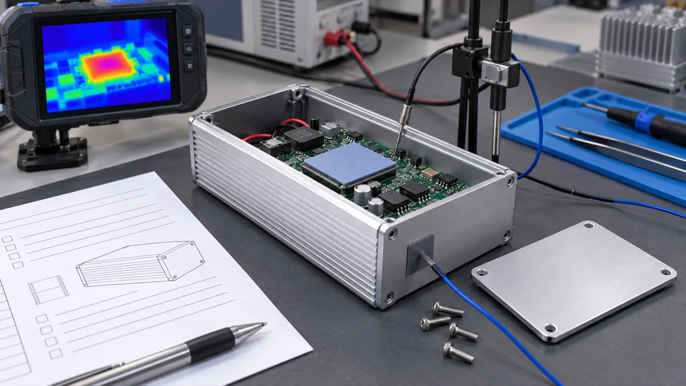
Prototype tests should use the real assembly path and operating conditions.
- Inspect pad contact after assembly. Look for evidence of full contact, displacement, local over-compression, or torn material without assuming visual appearance proves thermal performance.
- Measure at relevant points. Record component, enclosure, and ambient temperatures at defined operating states, including any installation orientation that affects cooling.
- Repeat closure checks. Confirm panel and connector alignment and check whether fastening distorts the PCB or changes the gap.
- Capture the test revision. Record the enclosure drawing, PCB revision, pad part, assembly method, and test conditions alongside the result.
If the prototype misses its target, change one defined part of the path and retest. An unpowered fit sample cannot validate heat performance.
What should be frozen before pilot production and repeat orders?
Freeze the geometry, pad specification, finish requirement, inspection method, and approved sample reference only after both fit and powered thermal tests meet the customer's defined criteria. This creates a clear basis for a pilot build and later repeat purchases.
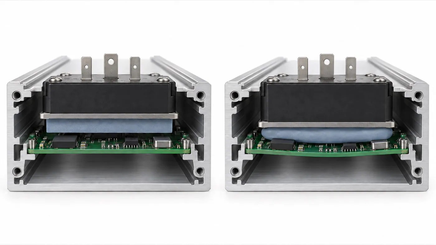
The approved build should preserve contact without loading the board beyond its design limits.
- Release one controlled package. Link enclosure drawing, PCB revision, pad part, finish specification, and acceptance notes.
- Define change triggers. A new component height, PCB thickness, profile, pad, or fastening arrangement calls for renewed gap and temperature review.
- Compare the pilot to the approved sample. Check functional dimensions and visible finish before using the pilot as a repeat-order baseline.
The enclosure supplier can support sample, pilot, and repeat supply against confirmed requirements. The customer remains responsible for electronics assembly and final system performance verification.
Conclusion
An effective aluminum enclosure thermal pad interface starts with a continuous heat path and a controlled assembled gap, then uses a compatible profile, suitable contact land, product-specific pad data, and a representative powered test. Prepare the PCB and enclosure drawings, component heights, pad candidate, mounting arrangement, operating conditions, and target quantity; the enclosure RFQ information guide can help organize the package before a supplier assesses the manufacturing route.
References
[1] Henkel, Thermal Interface Selection Guide. Product-specific information on gap-pad conformity, final thickness, pressure, and interface performance.
[2] Analog Devices, Thermal Characterization of IC Packages. Explanation of package and system thermal paths.